
Introduction
The 3D stacking market is emerging as a transformative segment within the semiconductor and electronics industry. 3D stacking technology involves vertically stacking multiple layers of integrated circuits to enhance performance, reduce power consumption, and optimize space utilization. This advanced packaging technique is increasingly being adopted to meet the growing demand for high-performance computing, miniaturization, and efficient data processing.
As modern applications such as artificial intelligence, data centers, and high-speed communication systems require enhanced computational capabilities, traditional 2D chip designs are reaching their limitations. 3D stacking provides a viable solution by enabling higher density and improved interconnectivity. The technology is gaining traction across various sectors, including consumer electronics, automotive, healthcare, and telecommunications.
The increasing adoption of advanced semiconductor technologies and the continuous push toward smaller, faster, and more efficient devices are driving the growth of the 3D stacking market. Furthermore, innovations in through-silicon via technology and wafer-level packaging are enhancing the feasibility and scalability of 3D stacking solutions.
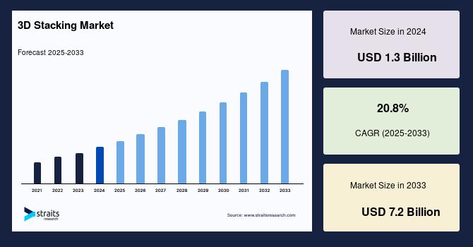
The global 3D stacking market size was valued at USD 1.65 billion in 2024.
It is expected to reach from USD 1.99 billion in 2025 to USD 9.48 billion in 2033, growing at a CAGR of 20.8% over the forecast period (2025-2033).
Get Full Report Now: https://straitsresearch.com/report/3d-stacking-market
Market Drivers and Challenges
Market Drivers
One of the primary drivers of the 3D stacking market is the increasing demand for high-performance and energy-efficient electronic devices. As applications such as artificial intelligence and machine learning continue to expand, the need for advanced semiconductor solutions is growing rapidly.
The trend toward miniaturization in consumer electronics is also fueling the adoption of 3D stacking technology. Manufacturers are seeking ways to integrate more functionality into smaller devices, and 3D stacking offers a compact and efficient solution.
The growing demand for high-speed data processing in data centers and cloud computing environments is another significant factor driving market growth. 3D stacking enables faster data transfer and improved system performance, making it ideal for these applications.
Additionally, advancements in semiconductor manufacturing technologies, including through-silicon vias and wafer bonding techniques, are enhancing the reliability and scalability of 3D stacking solutions.
Get Your Sample Report Here: https://straitsresearch.com/report/3d-stacking-market/request-sample
Market Challenges
Despite its advantages, the 3D stacking market faces several challenges. One of the key challenges is the high cost associated with advanced manufacturing processes. The complexity of stacking multiple layers of integrated circuits requires significant investment in technology and infrastructure.
Thermal management is another major concern. As multiple layers are stacked, heat dissipation becomes more challenging, which can impact device performance and reliability.
Design complexity also poses a challenge for manufacturers. Developing efficient and reliable 3D stacked architectures requires specialized expertise and advanced design tools.
Additionally, yield issues during manufacturing can affect production efficiency and increase costs, limiting widespread adoption in certain applications.
Market Segmentation
By Technology
The 3D stacking market is segmented into through-silicon via, monolithic 3D integration, and others.
Through-silicon via technology holds a significant share due to its ability to provide high-density interconnections between stacked layers. This technology is widely used in advanced semiconductor packaging.
Monolithic 3D integration is gaining attention as it enables the integration of multiple layers on a single substrate, offering improved performance and reduced latency.
Other technologies include emerging methods that enhance stacking efficiency and reliability.
By Device Type
The market is segmented into memory devices, MEMS/sensors, LEDs, imaging devices, and others.
Memory devices dominate the market due to increasing demand for high-capacity and high-speed memory solutions in computing and data storage applications.
MEMS and sensors are also significant segments, benefiting from compact designs and improved functionality offered by 3D stacking.
LEDs and imaging devices are increasingly adopting this technology to enhance performance and reduce form factors.
By End-User
The market includes consumer electronics, telecommunications, automotive, healthcare, and others.
Consumer electronics represent the largest segment due to high demand for smartphones, tablets, and wearable devices.
Telecommunications is another key segment, driven by the need for high-speed data transmission and network infrastructure.
The automotive sector is adopting 3D stacking for advanced driver-assistance systems and autonomous vehicles.
Healthcare applications include medical imaging and diagnostic devices, where compact and efficient designs are essential.
Regional Analysis
North America
North America holds a significant share of the 3D stacking market due to strong presence of semiconductor companies and advanced technological infrastructure.
Europe
Europe is witnessing steady growth, supported by increasing adoption of advanced electronics and automotive technologies.
Asia-Pacific
Asia-Pacific is expected to dominate the market during the forecast period due to the presence of major semiconductor manufacturers and high demand for consumer electronics.
Rest of the World
Other regions are gradually adopting 3D stacking technologies as awareness and technological capabilities increase.
Top Players Analysis
- Intel Corporation – Intel Corporation is a leading player in semiconductor innovation, focusing on advanced packaging technologies including 3D stacking to enhance computing performance.
- Samsung Electronics Co., Ltd. – Samsung Electronics is a key player offering advanced memory and semiconductor solutions, leveraging 3D stacking technology for improved efficiency.
- Taiwan Semiconductor Manufacturing Company Limited – TSMC is a major semiconductor foundry specializing in advanced chip manufacturing and 3D integration technologies.
- Micron Technology, Inc. – Micron Technology focuses on memory and storage solutions, utilizing 3D stacking to deliver high-performance products.
- SK Hynix Inc. – SK Hynix is known for its advanced memory technologies, incorporating 3D stacking for improved capacity and speed.
- Toshiba Corporation – Toshiba Corporation provides semiconductor solutions with a focus on innovation and performance enhancement through advanced technologies.
- Broadcom Inc. – Broadcom Inc. offers a wide range of semiconductor and infrastructure software solutions, integrating 3D stacking for enhanced functionality.
Conclusion
The 3D stacking market is poised for significant growth, driven by increasing demand for high-performance and compact electronic devices. The technology offers numerous advantages, including improved performance, reduced power consumption, and efficient space utilization.
While challenges such as high costs and thermal management issues remain, ongoing advancements in semiconductor technologies are expected to address these concerns. The market presents substantial opportunities for growth, particularly in emerging applications such as artificial intelligence and autonomous systems.
As industries continue to push the boundaries of innovation, 3D stacking will play a crucial role in shaping the future of semiconductor technology and enabling next-generation electronic devices.
FAQs
What is 3D stacking technology?
3D stacking is a semiconductor technology that involves vertically stacking multiple layers of integrated circuits to improve performance and efficiency.
What is driving the growth of the 3D stacking market?
The market is driven by demand for high-performance computing, miniaturization of devices, and advancements in semiconductor technologies.
What are the key challenges in this market?
Major challenges include high manufacturing costs, thermal management issues, and design complexity.
Which segment dominates the market?
Memory devices dominate due to increasing demand for high-capacity and high-speed storage solutions.
Which region leads the market?
Asia-Pacific is expected to dominate due to strong semiconductor manufacturing presence.
About Us:
Straits Research is a leading research and intelligence organisation, specialising in research, analytics, and advisory services, along with providing business insights & research reports.
Contact Us:
Email: sales@straitsresearch.com
Tel: +1 646 905 0080 (U.S.), +44 203 695 0070 (U.K.)